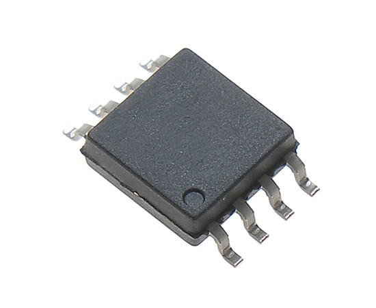
AT45DB021E-SHN Adesto
| Case: | SOIC08 |
| Frequency: | 70MHz |
| Supply voltage range: | 1,65~3,6V |
| Manufacturer: | Adesto |
| FLASH memory: | 256kB |
| Architecture: | 8-bit |
| Operating temperature (range): | -40°C ~ 85°C |
| Quantity of pcs. | 2000+ (Need a significantly larger quantity? Ask for price). |
|---|---|
| Net price (EUR) | 0,7810 |
| Quantity of pcs. | 180+ (Need a significantly larger quantity? Ask for price). |
|---|---|
| Net price (EUR) | 0,7810 |
| Quantity of pcs. | 5+ (Need a significantly larger quantity? Ask for price). |
|---|---|
| Net price (EUR) | 0,8955 |
| Case: | SOIC08 |
| Frequency: | 70MHz |
| Supply voltage range: | 1,65~3,6V |
| Manufacturer: | Adesto |
| FLASH memory: | 256kB |
| Architecture: | 8-bit |
| Operating temperature (range): | -40°C ~ 85°C |
AT45DB021E - Serial DataFlash memory with SPI compatibility, 2 megabit capacity (+ additional 64 kilobits), powered as low as 1.65 V.
Features:
• Single supply voltage range: 1.65 V – 3.6 V
• SPI interface compatibility
- Supports SPI modes 0 and 3
- RapidSTM-compatible
• Continuous read from entire memory
- Up to 85 MHz
- Low-power read mode to 15 MHz
- Maximum read access time (clock-to-output, tV) 6 ns
• User-definable page size
- 256 bytes per page
- 264 bytes per page (default value)
- Option to factory-set page size to 256 bytes
• One SRAM buffer (256/264 bytes)
• Flexible programming options
- Byte-level or page-level programming (from 1 to 256/264 bytes)
- Write-buffering
- Buffer page copy to main memory
• Flexible erasure options
- Erase pages (256/264 bytes)
- Erase blocks (2 kB)
- Erase sectors (32 kB)
- Erase entire chip (2 Mb)
• Advanced data protection mechanisms
- Individual sector protection
- Ability to lock sectors to read-only mode
• 128-byte security register, one-time programmable
- 64 bytes containing a factory-programmed unique identifier
- 64 bytes for user data
• Hardware and software reset options
• Manufacturer and device ID readout per JEDEC standard
• Low power dissipation
- Ultra-deep shutdown current: 200 nA (typical)
- Deep shutdown current: 3 µA (typical)
- Standby current: 25 µA (typical at 20 MHz)
- Read current: 4.5 mA (typical)
• Endurance: at least 100,000 program/erase cycles per page
• Data retention: 20 years
• Industrial temperature range compliance
• Eco-friendly variants available (lead-free, halogen-free, RoHS-compliant)
- 8-pin SOIC package (0.150" width, 0.208" length)
- 8-pin ultra-thin DFN package (5 x 6 x 0.6 mm)
- 9-ball ultra-thin UBGA package (6 x 6 x 0.6 mm)
Description
Adesto® AT45DB021E is a serial Flash memory with sequential access, powered by a voltage as low as 1.65 V. It is ideal for a wide range of devices that require storage of voice, images, program code, or data. AT45DB021E is also compatible with the RapidS serial interface, which is crucial for applications requiring very high performance. The 2,162,688 bits of memory are divided into 1024 pages, each consisting of 256 or 264 bytes. In addition to main memory, AT45DB021E also includes an SRAM buffer of 256/264 bytes. It can be used as extra memory for paging, and with its three-stage operation (read-modify-write), it facilitates emulating EEPROM memory, providing access to contents at the bit or byte level. Unlike traditional Flash memories with random access, which employ parallel interfaces and multiple address lines, Adesto DataFlash® uses a serial interface with sequential access.
The simplicity of its design leads to a drastic reduction in the number of required pins, simplifies routing, increases system reliability, reduces EMI interference, and allows the memory to be housed in a small package. The device has been optimized for commercial and industrial solutions, where high component density, fewer leads, low supply voltage, and low power consumption are key factors.
The AT45DB021E does not require high-voltage programming, enabling fast in-system reprogramming. Erasure and programming, as well as reading, take place with a supply voltage range from 1.65 V to 3.6 V. Memory access is enabled via the Chip Select (CS) pin and uses a three-wire interface: Serial Input (SI), Serial Output (SO), and Serial Clock (SCK). Timing control for all programming and erasure operations is automated.

