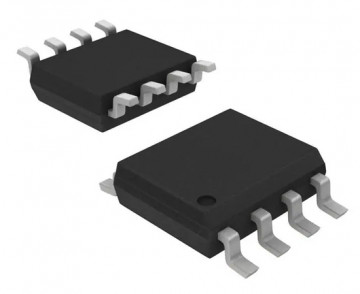
AT45DB041E-SSHN-B
| Case: | SOP08 |
| Frequency: | 85MHz |
| Supply voltage range: | 1,65~3,6V |
| Manufacturer: | Adesto |
| FLASH memory: | 512kB |
| Architecture: | 8-bit |
| Operating temperature (range): | -40°C ~ 85°C |
| Quantity of pcs. | 1+ | 5+ | 20+ | 100+ | 300+ |
|---|---|---|---|---|---|
| Net price (EUR) | 1,6650 | 1,2334 | 1,0801 | 1,0023 | 0,9787 |
| Quantity of pcs. | 1+ | 5+ | 20+ | 100+ | 300+ |
|---|---|---|---|---|---|
| Net price (EUR) | 1,6650 | 1,2334 | 1,0801 | 1,0023 | 0,9787 |
| Quantity of pcs. | 5+ (Need a significantly larger quantity? Ask for price). |
|---|---|
| Net price (EUR) | 0,9787 |
| Quantity of pcs. | 7+ (Need a significantly larger quantity? Ask for price). |
|---|---|
| Net price (EUR) | 0,9787 |
| Quantity of pcs. | 4000+ (Need a significantly larger quantity? Ask for price). |
|---|---|
| Net price (EUR) | 0,9787 |
| Case: | SOP08 |
| Frequency: | 85MHz |
| Supply voltage range: | 1,65~3,6V |
| Manufacturer: | Adesto |
| FLASH memory: | 512kB |
| Architecture: | 8-bit |
| Operating temperature (range): | -40°C ~ 85°C |
| SPI interface: | YES |
AT45DB041E - Serial, SPI-compatible DataFlash memory with a capacity of 4 megabits (+ additional 128 kilobits),
powered from 1.65 V.
Features:
• Single supply voltage range from 1.65 V – 3.6 V
• SPI interface compatibility
- Supports SPI modes 0 and 3
- Compatibility with RapidS™
• Ability to read the entire memory contents in continuous mode
- Up to 85 MHz
- Low-power read mode up to 15 MHz
- Maximum read time (clock-to-output, tV) 6 ns
• User-selectable page size
- 256 bytes per page
- 264 bytes per page (default value)
- Option for factory preset to 256 bytes per page
• One SRAM data buffer (256/264 bytes)
• Flexible programming capabilities
- Direct programming of main memory at the byte or page level (from 1 to 256/264 bytes)
- Write buffering
- Buffering page copy to main memory
• Flexible erase options
- Page erase (256/264 bytes)
- Block erase (2 kB)
- Sector erase (64 kB)
- Chip erase (4 Mb)
• Advanced hardware and software data protection mechanisms
- Protection of individual sectors
- Ability to lock individual sectors (switch them to read-only mode)
• 128-byte security register that can be programmed only once
- 64 bytes with a factory-assigned unique identifier
- 64 bytes for user data
• Hardware and software reset
• Manufacturer and device ID read according to the JEDEC standard
• Low power dissipation
- Ultra-deep power-down mode current of 400 nA (typical)
- Deep power-down mode current of 3 μA (typical)
- Standby mode current of 25 μA (typical at 20 MHz)
- Read mode current of 11 mA (typical)
• Endurance: at least 100,000 program/erase cycles per page
• Data retention: 20 years
• Industrial operating temperature range compatibility
• Availability of eco-friendly (lead-free, halogen-free, RoHS-compliant) versions
- 8-pin SOIC package (width 0.150ʺ, length 0.208")
- 8-pin ultra-thin DFN package (5 x 6 x 0.6 mm)
Description
Adesto® AT45DB041E is a serial Flash memory with sequential access, powered by a voltage of 1.65 V. It is an ideal choice for a wide range of devices that require storing voice, images, program code, or data. AT45DB041E is also compatible with the RapidS serial interface, which is important for applications requiring very high-speed performance. The 4,194,304 bits of memory are divided into 2,048 pages, each consisting of 256 or 264 bytes. In addition to the main memory, AT45DB041E also includes a single 256/264-byte SRAM buffer. This buffer can serve as additional page memory, and thanks to its three-phase operation in read-modify-write mode, it allows for easy implementation of EEPROM emulation, providing access to the contents at the bit or byte level. Unlike traditional Flash memories with random access, multiple address lines, and parallel interfaces, Adesto DataFlash® uses a serial interface and sequential access.
Its simplicity leads to a significant reduction in the number of required pins, simplifies routing design, increases system reliability, reduces EMI interference, and allows the memory to be placed in a compact package. The device has been optimized for use in a variety of commercial and industrial solutions, where high component density, a small number of pins, low supply voltage, and low energy consumption are essential.
AT45DB041E does not require high-voltage programming, allowing for fast in-system reprogramming. Erasing, programming, and reading are performed with supply voltages ranging from 1.65 V to 3.6 V. The AT45DB041E is activated via the Chip Select (CS) pin and is accessed using a three-wire interface: Serial Input (SI), Serial Output (SO), and Serial Clock (SCK). Timing for all programming and erase operations is managed automatically.

