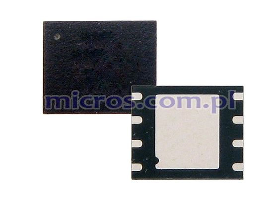
AT45DB081E-MHN
| Case: | uDFN08 |
| Frequency: | 85MHz |
| Manufacturer: | Adesto |
| Supply voltage range: | 1.7~3.6V |
| FLASH memory: | 1MB |
| Architecture: | 8-bit |
| Operating temperature (range): | -40°C ~ 85°C |
| Quantity of pcs. | 1+ | 3+ | 10+ | 40+ | 200+ |
|---|---|---|---|---|---|
| Net price (EUR) | 1,6656 | 1,3282 | 1,1362 | 1,0307 | 0,9792 |
| Quantity of pcs. | 1+ | 5+ | 20+ | 100+ | 300+ |
|---|---|---|---|---|---|
| Net price (EUR) | 1,6656 | 1,2345 | 1,0799 | 1,0026 | 0,9792 |
| Quantity of pcs. | 570+ (Need a significantly larger quantity? Ask for price). |
|---|---|
| Net price (EUR) | 0,9792 |
| Case: | uDFN08 |
| Frequency: | 85MHz |
| Manufacturer: | Adesto |
| Supply voltage range: | 1.7~3.6V |
| FLASH memory: | 1MB |
| Architecture: | 8-bit |
| Operating temperature (range): | -40°C ~ 85°C |
AT45DB081E - serial SPI-compatible DataFlash memory with a capacity of 8 megabits (+ additional 256 kilobits),
powered from as low as 1.7 V.
Features:
• Single supply voltage range from 1.7 V to 3.6 V
• SPI interface compatibility
- supports SPI modes 0 and 3
- compatible with RapidS™
• Continuous read of entire memory content
- up to 133 MHz
- low power read mode up to 20 MHz
- maximum read time (clock-to-output, tV) 6 ns
• User-configurable page size
- 256 bytes per page
- 264 bytes per page (default value)
- factory default setting for page size of 256 bytes
• Single SRAM buffer (256/264 bytes)
• Flexible programming options
- direct programming at the byte or page level (from 1 to 256/264 bytes)
- write buffering
- page copy buffering to main memory
• Flexible erase options
- page erase (256/264 bytes)
- block erase (2 kB)
- sector erase (64 kB)
- chip erase (8 Mb)
• Advanced hardware and software data protection mechanisms
- protection of individual sectors
- ability to lock individual sectors (set to read-only mode)
• Security register of 128 bytes, programmable only once
- 64 bytes factory programmed with a unique identifier
- 64 bytes for user data
• Hardware and software reset
• Manufacturer and device identifier readout compliant with JEDEC standard
• Low dissipated power
- ultra deep sleep current: 400 nA (typical)
- deep sleep current: 4.5 μA (typical)
- standby current: 25 μA (typical at 20 MHz)
- read current: 8 mA (typical)
• Endurance: at least 100,000 program/erase cycles per page
• Data retention: 20 years
• Industrial temperature range compatibility
• Available in environmentally friendly variants (lead-free, halogen-free, RoHS compliant)
- 8-pin SOIC package (0.150" width, 0.208" length)
- 8-pin ultra-thin DFN package (5 x 6 x 0.6 mm)
Description
Adesto® AT45DB081E is a serial flash memory with sequential access, powered by a voltage range from 1.7 V. It is an ideal choice for a wide range of applications that require storing voice, images, program code, or data. AT45DB081E is also compatible with the RapidS serial interface, making it suitable for applications that require very high-speed operation. The 8,650,752 bits of memory are divided into 4,096 pages, each consisting of 256 or 264 bytes. In addition to the main memory, AT45DB081E also contains a 256/264-byte SRAM buffer, which can serve as additional paging memory. With its three-step operation, read-modify-write, it can easily emulate an EEPROM, offering access to its content at the individual bit or byte level. Unlike traditional Flash memories with random access and parallel interfaces, Adesto DataFlash® memories utilize a serial interface with sequential access.
Its simplicity translates into a drastic reduction in the number of required pins, easing PCB layout design, increasing system reliability, reducing EMI interference, and allowing the memory to be housed in a compact package. The device has been optimized for use in numerous commercial and industrial applications where high component density, fewer pins, low supply voltage, and low energy consumption are crucial.
AT45DB081E does not require high-voltage programming, allowing for fast in-circuit reprogramming. Erase and programming operations, as well as data reads, are carried out with supply voltages between 1.7 V and 3.6 V. The memory is activated via the Chip Select (CS) pin and accessed using a three-wire interface: Serial Input (SI), Serial Output (SO), and Serial Clock (SCK). The timing requirements for all programming and erase operations are handled automatically.

