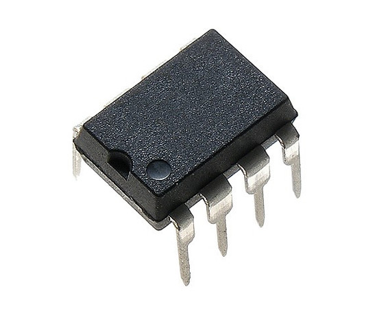
LM6172IN
| Nominal voltage: | 2,75V ~ 18V |
| Bandwidth: | 100MHz |
| Vaoltage rise speed: | 3000V/us |
| Case: | PDIP08 |
| Manufacturer: | Texas Instruments |
| Operating temperature (range): | -40°C ~ 85°C |
| Integrated circuit type: | Operational amplifier |
| Nominal voltage: | 2,75V ~ 18V |
| Bandwidth: | 100MHz |
| Vaoltage rise speed: | 3000V/us |
| Case: | PDIP08 |
| Manufacturer: | Texas Instruments |
| Operating temperature (range): | -40°C ~ 85°C |
| Integrated circuit type: | Operational amplifier |
| Mounting: | THT |
| Number of channels: | 2 |
The LM6172IN Circuit contains two very fast voltage-feedback operational amplifiers with low distortion and low current consumption. The circuit uses complementary bipolar technology (also used in current-feedback amplifiers).
The LM6172 offers a wide range of supply voltages, which can be both symmetric and asymmetric: ±15V (or 0 to 30V) for applications requiring a wide range of output voltage changes, or ±3V (or 0 to 6V) for applications in portable devices, for example.
Selected Properties [for VCC =±15V and Ta = 25°C]
- Number of amplifiers: 2;
- Common-mode input voltage range: ±13.5V;
- Output voltage swing: ±13.2V;
- Input offset voltage: 0.4mV;
- Temperature drift of offset voltage: 6µV/°C;
- Input bias current: 1.2µA;
- Input offset current: 20nA;
- Current consumption: 2.3mA per amplifier;
- Output current: 90mA;
- Gain-bandwidth product (GBW): 160MHz;
- Bandwidth: 100MHz;
- Output slew rate (SR): 3000V/µs;
- Settling time: 65ns;
- Noise voltage density at input: 12nV/√Hz;
- Supply voltage:
- Symmetric: ±2.75 to ±18V;
- Asymmetric: 5.5 to 36V;
- Operating temperature: -40 to 85°C;
- Package type: PDIP08.
Typical Applications: Pulse technology, TV systems, buffer for A/D and D/A converters, peak detector.
Pinout:
Practical Notes from the Manufacturer:
- If the amplifier is used with a capacitive load, there is a risk of the circuit oscillating and causing unwanted output oscillations. It is recommended to increase the phase margin by adding a 50Ω resistor in series with the amplifier output.
- If a very fast pulse is applied to the amplifier input, output overshoot may occur. It is recommended to limit the speed by adding a 1kΩ resistor in series with the amplifier input.
- When designing the PCB, it is recommended to follow high-frequency circuit design rules. Pay attention to proper trace routing, power decoupling, impedance matching, and grounding.


